Microscope
A microscope (from the Ancient Greek: μικρός, mikrós, "small" and σκοπεῖν, skopeîn, "to look" or "see") is an instrument used to see objects that are too small to be seen by the naked eye. Microscopy is the science of investigating small objects and structures using such an instrument. Microscopic means invisible to the eye unless aided by a microscope.
There are many types of microscopes, and they may be grouped in different ways. One way is to describe the way the instruments interact with a sample to create images, either by sending a beam of light or electrons to a sample in its optical path, or by scanning across, and a short distance from, the surface of a sample using a probe. The most common microscope (and the first to be invented) is the optical microscope, which uses light to pass through a sample to produce an image. Other major types of microscopes are the fluorescence microscope, the electron microscope (both, the transmission electron microscope and the scanning electron microscope) and the various types of scanning probe microscopes.[1]

Evolution of spatial resolution achieved with optical, transmission (TEM) and aberration-corrected electron microscopes (ACTEM).[25]
Microscopes can be separated into several different classes. One grouping is based on what interacts with the sample to generate the image, i.e., light or photons (optical microscopes), electrons (electron microscopes) or a probe (scanning probe microscopes). Alternatively, microscopes can be classified based on whether they analyze the sample via a scanning point (confocal optical microscopes, scanning electron microscopes and scanning probe microscopes) or analyze the sample all at once (wide field optical microscopes and transmission electron microscopes).
Wide field optical microscopes and transmission electron microscopes both use the theory of lenses (optics for light microscopes and electromagnet lenses for electron microscopes) in order to magnify the image generated by the passage of a wavetransmitted through the sample, or reflected by the sample. The waves used are electromagnetic (in optical microscopes) or electron beams (in electron microscopes). Resolution in these microscopes is limited by the wavelength of the radiation used to image the sample, where shorter wavelengths allow for a higher resolution.[20]
Scanning optical and electron microscopes, like the confocal microscope and scanning electron microscope, use lenses to focus a spot of light or electrons onto the sample then analyze the signals generated by the beam interacting with the sample. The point is then scanned over the sample to analyze a rectangular region. Magnification of the image is achieved by displaying the data from scanning a physically small sample area on a relatively large screen. These microscopes have the same resolution limit as wide field optical, probe, and electron microscopes.
Scanning probe microscopes also analyze a single point in the sample and then scan the probe over a rectangular sample region to build up an image. As these microscopes do not use electromagnetic or electron radiation for imaging they are not subject to the same resolution limit as the optical and electron microscopes described above.
Optical
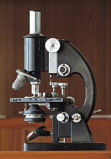
The most common type of microscope (and the first invented) is the optical microscope. This is an optical instrument containing one or more lenses producing an enlarged image of a sample placed in the focal plane. Optical microscopes have refractive glass (occasionally plastic or quartz), to focus light on the eye or on to another light detector. Mirror-based optical microscopes operate in the same manner. Typical magnification of a light microscope, assuming visible range light, is up to 1250x with a theoretical resolution limit of around 0.250 micrometres or 250 nanometres.[20] This limits practical magnification to ~1500x. Specialized techniques (e.g., scanning confocal microscopy, Vertico SMI) may exceed this magnification but the resolution is diffractionlimited. The use of shorter wavelengths of light, such as ultraviolet, is one way to improve the spatial resolution of the optical microscope, as are devices such as the near-field scanning optical microscope.
Sarfus is a recent optical technique that increases the sensitivity of a standard optical microscope to a point where it is possible to directly visualize nanometric films (down to 0.3 nanometre) and isolated nano-objects (down to 2 nm-diameter). The technique is based on the use of non-reflecting substrates for cross-polarized reflected light microscopy.
Ultraviolet light enables the resolution of microscopic features as well as the imaging of samples that are transparent to the eye. Near infrared light can be used to visualize circuitry embedded in bonded silicon devices, since silicon is transparent in this region of wavelengths.
In fluorescence microscopy many wavelengths of light ranging from the ultraviolet to the visible can be used to cause samples to fluoresce which allows viewing by eye or with specifically sensitive cameras.
Phase contrast microscopy is an optical microscopy illumination technique in which small phase shifts in the light passing through a transparent specimen are converted into amplitude or contrast changes in the image.[20] The use of phase contrast does not require staining to view the slide. This microscope technique made it possible to study the cell cycle in live cells.
The traditional optical microscope has more recently evolved into the digital microscope. In addition to, or instead of, directly viewing the object through the eyepieces, a type of sensor similar to those used in a digital camera is used to obtain an image, which is then displayed on a computer monitor. These sensors may use CMOS or charge-coupled device (CCD) technology, depending on the application.
Digital microscopy with very low light levels to avoid damage to vulnerable biological samples is available using sensitive photon-counting digital cameras. It has been demonstrated that a light source providing pairs of entangled photons may minimize the risk of damage to the most light-sensitive samples. In this application of ghost imagingto photon-sparse microscopy, the sample is illuminated with infrared photons, each of which is spatially correlated with an entangled partner in the visible band for efficient imaging by a photon-counting camera.[26]
Electron
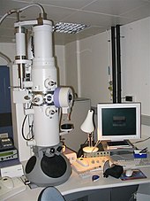
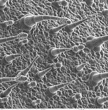
The two major types of electron microscopes are transmission electron microscopes(TEMs) and scanning electron microscopes(SEMs).[20][21] They both have series of electromagnetic and electrostatic lenses to focus a high energy beam of electrons on a sample. In a TEM the electrons pass through the sample, analogous to basic optical microscopy.[20] This requires careful sample preparation, since electrons are scattered strongly by most materials.[21] The samples must also be very thin (50-100 nm) in order for the electrons to pass through it.[20][21]Cross-sections of cells stained with osmium and heavy metals reveal clear organelle membranes and proteins such as ribosomes.[21] With a 0.1 nm level of resolution, detailed views of viruses (20-300 nm) and a strand of DNA (2 nm in width) can be obtained.[21] In contrast, the SEM has raster coils to scan the surface of bulk objects with a fine electron beam. Therefore, the specimen do not necessarily need to be sectioned, but require coating with a substance such as a heavy metal.[20] This allows three-dimensional views of the surface of samples.[20][21]
Scanning probe
The different types of scanning probe microscopes arise from the many different types of interactions that occur when a small probe of some type is scanned over and interacts with a specimen. These interactions or modes can be recorded or mapped as function of location on the surface to form a characterization map. The three most common types of scanning probe microscopes are atomic force microscopes(AFM), near-field scanning optical microscopes (MSOM or SNOM, scanning near-field optical microscopy), and scanning tunneling microscopes (STM).[27] An atomic force microscope has a fine probe, usually of silicon or silicon nitride, attached to a cantilever; the probe is scanned over the surface of the sample, and the forces that cause an interaction between the probe and the surface of the sample are measured and mapped. A near-field scanning optical microscope is similar to an AFM but its probe consists of a light source in an optical fiber covered with a tip that has usually an aperture for the light to pass through. The microscope can capture either transmitted or reflected light to measure very localized optical properties of the surface, commonly of a biological specimen. Scanning tunneling microscopes have a metal tip with a single apical atom; the tip is attached to a tube through which a current flows.[28] The tip is scanned over the surface of a conductive sample until a tunneling current flows; the current is kept constant by computer movement of the tip and an image is formed by the recorded movements of the tip.[27]
Other types
Scanning acoustic microscopes use sound waves to measure variations in acoustic impedance. Similar to Sonar in principle, they are used for such jobs as detecting defects in the subsurfaces of materials including those found in integrated circuits. On February 4, 2013, Australian engineers built a "quantum microscope" which provides unparalleled
REFRENCE higherschool
precision.[29

First atomic force microscope
- ^ Characterization and Analysis of Polymers. Hoboken, N.J.: Wiley-Interscience. 2008. ISBN 978-0-470-23300
by ajay yadavhigherschoolhigherschool


Comments
Post a Comment